BGA Voiding
X-Ray Radiography Inspection
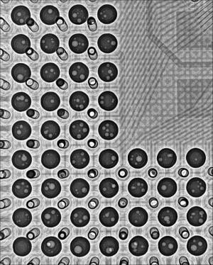
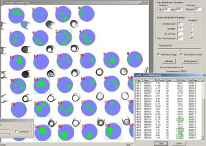
This report contains images taken of the BGAs on the two boards provided. There are no significant defects present, however, significant voiding is present throughout the two parts. The last image shows a BGA analysis performed on one of the worst areas of voiding. The analysis shows voiding greater than 15%, but less than 20%.
When run, this feature shows voiding in the solder joints as well as background features such as traces and vias, all within the same image.
IPC-610 acceptability criterion for voiding in IPC-610 is currently <25% void area on transmission x-ray. The voids in this joint are not localized at the component or PWB interface but are evenly distributed throughout the joint. Current research seems to indicate that in this situation, the voiding is unlikely to have a negative effect on reliability. It is, however, a process indicator. The joint voiding, a product of the manufacturing process, has a root cause(s) and one has to optimize the process to reduce the occurrence of the voids.
Gideon Analytical Labs has the equipment to handle your needs in the electronic industry. Call us with your needs.
Ball Grid Array
Voiding on BGA