Design Debug
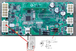
This picture shows the entire printed circuit board with epoxy encapsulated. This type of encapsulation coating is great for automotive electronic applications where vibration and debris can be minimized, but it will prevent cooling efficiency since the component surface area will not radiate heat by convection to ambient air, and it can prevent simple follow-up rework, probing, debug, and failure analysis.
Correctly left out of the epoxy area are connectors, terminal screws, and any power devices. Physical inspection reveals the several burnt components which were consistent with electrical overload. The environmental degradation of the component film, end cap connections, and epoxy encapsulant chemical interactions were eliminated as the cause since no other component degradation exists, including identical components in many neighboring circuit locations. The epoxy has disbonded from the PCB surface which is a result of the heat, pressure, and moisture generated as the component failed.
After review of electrical schematics, the burnt components were carrying 3 times the wattage that was supposed to be present. This extra heat, since it cannot be dissipated, burned the components.
Gideon Analytical Labs has EE engineers who are at the top of their game in designing circuits and diagnosing design flaws. Gideon Analytical Labs could correct your designs also and correct the field failures.
PCB with component usage issues