Synchronous Buck Driver TI UCC27223PWP Failure Analysis
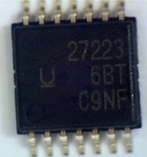
Gideon Analytical Labs received two failed TI UCC27223PWP and three vintage devices for comparison. Two 14 pin Dip TI UCC27223PWP functional failures were sent from assemblies. The UCC27223 is a high-speed synchronous buck driver for thigh-efficiency lower-output voltage designs. Using PredictiveGate Drive (PGD) control technology, these drivers reduce diode conduction and reverse recovery losses in the synchronous rectifier MOSFET(s). The UCC27223 has an enable pin that controls the operation of both outputs. A logic latch, which keeps both outputs low until the first PWM input pulse comes in, is included. The RDS(on) of the SR pull-down sourcing device is minimized for higher frequency operations. This closed loop feedback system detects body-diode conduction and adjusts dead time delays to minimize the conduction time interval. This virtually eliminates body-diode conduction while adjusting for temperature, load-dependent delays, and for different MOSFETs. Precise gate timing at the nanosecond level reduces the reverse recovery time of the synchronous rectifier MOSFET body-diode, reducing reverse recovery losses seen in the main (high-side) MOSFET. The lower junction temperature in the low-side MOSFET increases product reliability. Since the power dissipation is minimized, a higher switching frequency can also be used, allowing for smaller component sizes.
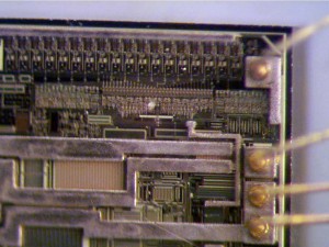
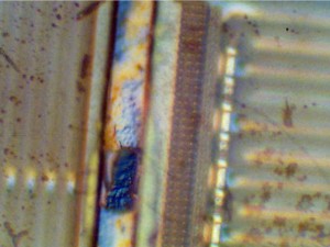
As much information as possible is obtained from the customer to complete the component failure analysis. The devices were tested on a curve tracer for any electrical discrepancies that could be determined before decapsulating the package. The specification refers to the R-enbl resistor as inserted between the Vdd and the ENBL pin inside the circuitry. To measure this, 14V is applied to Vdd and measured to enable pin 2. On a good device, this measures right around 114Kohms. The specification indicates anything between 75 and 150Kohms is acceptable. On the failed units, when this was done an open circuit is evident between pins 2 and 3. Since pin Vdd is tied directly to the regular and has the output connected to VLO (pin4), we tried a 12V continuity test. The curve trace showed an open circuit. The devices are symptomatic of the same issues; they both have the 110Kohm resistor absent from the circuit and the VLO regulator is open to pin 4. At first, it was thought an electrical overcurrent was coming in the VLO pin over stressing the interconnects; thus opening up the resistor and the regulator from pin 4, VLO, however, on the second device demonstrates a clear electrical overstress on (EOS) on pin 6, the ground pin beneath the pad area and the first perhaps an overstress exiting the regulator.
Gideon Analytical Labs can solve the problems that lead to either a circuit design change or identify a component or lead that has been overstressed of either voltage or current. In the current device, an overvoltage caused the burning. Call Gideon for your component failure analysis.

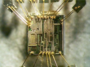
TI UCC27223PWP Die

TI UCC27223PWP Failed Area

ti-3

ti-4