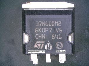
Failure Analysis of STMicroelectronics STW37N60DM2AG 600V MOSFETs
Gideon received six failed STMicroelectronics STW37N60DM2AG 600V MOSFETs for failure analysis. These high voltage N-channel Power MOSFET are part of the MDmesh™ DM2 fast recovery diode series. They offer a very low recovery charge (Qrr) and time (trr) combined with low RDS(on), rendering it suitable for the most demanding high-efficiency converters and ideal for bridge topologies and ZVS phase-shift converters. These were installed on an H-bridge with assured engineering support that there was no waveform overlapping during the transition. If these signals overlap, the MOSFETs will short circuit the supply, and a shoot-through condition will arise which will effectively cause the rapid discharge of the decoupling capacitors through the MOSFETs on every switching transition, thus dissipating a tremendous amount of heat through the silicon, a short, and a large current pulse.
The MOSFET is used to control the voltage and current flow between the source and drain. It works like a switch, and its function depends upon the MOS capacitor. The MOS capacitor is the central part of MOSFET. The silicon has a double diffused region. The source metal meets or contacts the N+ region, and this is diffused into a P region within the N drift region. Thus, the NPN arrangement. The surface below the field oxide layer, which is located between the source and drain terminal, can be inverted from p-type (2nd diffusion) to n-type by applying a positive gate voltage.
When a positive gate voltage is applied, the holes present under the field oxide layer are repelled deeper into the bulk silicon area, leaving an N channel in the P diffusion. Also, the positive voltage attracts the electrons into this repelled area, which opens a channel between the N+ source contact and the N-drift area across what was a P-region just under the gate oxide. This depletion region, as it is known, is now colonized with negative charges which accommodate the electron flow of current. In an enhancement type MOSFET, the gate turns on with gate voltage. In a depletion type MOSFET, the channel is entirely on with no gate voltage. If a voltage is now applied (enhanced type) between the drain and source, the current flows freely between the source and drain, and the gate voltage controls the electrons in the channel. The opposite is true if a negative voltage were applied. If a negative voltage is applied, a hole channel will be formed under the oxide layer and no current will flow.
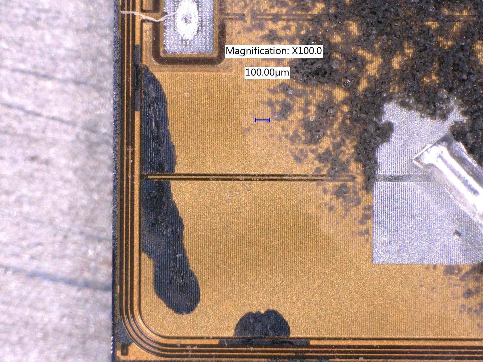
With the presence of carbon, caused by the pyrolysis of the epoxy in the anaerobic environment, the die shows signs of significant heat. The die surface could not be inspected because of tenacious adherence of the carbon to the polyimide cover coat. This carbon had to be removed without destroying the die surface. This was done using several chemicals. Several of the initial die showed a voltage spike from drain to source, and all terminals shorted. Usually, a shoot-through is expected when the die is exposed to excessive heat. How did it produce the heat? One must examine the circuit schematics and run waveforms capturing these transitions, measure the dv/dt, and observe any voltage spikes when and if they occur using an oscilloscope.
The MOSFET was connected to an oscilloscope to measure the dv/dt. The waveform was captured at 70V/ns, indicating a 20V higher rate than the manufacturers’ rating on the specification sheet. The drain-source voltage changes rapidly during turn-off; this caused a varying current to flow through the pn junction, both capacitance, and resistance. This excess current then causes a voltage drop across the base and emitter of the parasitic bipolar transistor (PBT). The PBT turns on if the voltage drop exceeds its base-emitter voltage to turn on.
Thus, another problem solved by the experts at Gideon! We can reverse bad engineering applications, perform testing to prove the outcome, redesign an old design, failure analyze the electrical components, determine the failure mode of the component and know-how that relates to the circuit design, perform waveform circuit diagnostics and much more. We also know the wear-out mechanisms, the induced failure mechanisms, and the causes of failures related to process, assembly, testing, installation, contamination, materials, metallurgy, and more. Call Gideon 845-255-5356.
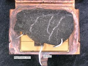
Carbonized epoxy from the generated heat

Spike through pin the right
Burned out section of the failure site

D-S Short
ST MOSFET
Failure site
Title