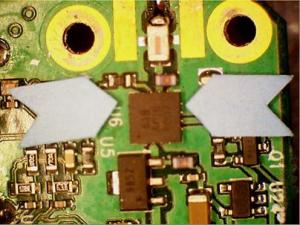
PCB with Amplifier Failed from EOS
Gideon Analytical Laboratories received a single MA COM MAAPSS0096 1 watt power amplifier for failure analysis. The device was thought to have some impedance issues.
The device was still attached to PCB on arrival, as displayed in the picture at the top left. The device was removed from the PCB and tested to find any indication of the condition of the internal circuitry. The MAAPSS0113 is a three stage power amplifier designed for Digitally Enhanced Cordless Telephone applications. The power amplifier is available in a lead-free 3 mm 12-lead PQFN plastic package. The MAAPSS0113 features an integrated power enable pin (5) for accurate ramp control and a separate power mode pin (2) for current savings in a low power mode state. Both control pins operate with 1.7 V logic. A voltage compensation circuit is also included for applications where the amplifier supply voltage is not regulated and is directly connected to the battery.
The leads were tested for any shorting and continuity issues. A new device showed no continuity between any of the pins as long as the input was not activated. When the failed device was tested, all the pins showed high impedance. When the package was pressed down physically, these two leads short and open back up when the pressure was released. Continuity testing was done using 7 volts and maximum power of .1 watts, thus limiting the current to about 15ua. The device was decapsulated.
The cloudy material is gallium arsenide that has under gone extensive acid exposure; it has essentially started to dissolve. This cloudy material is visible in the picture at the top right. Final results of the failure analysis were the caused by excessive power (surge current) coming in the Vdd pin electrically over whelmed several trace lines.
Failure analysis performed by Gideon Analytical Laboratories can be used by electronics companies in a numerous variety of ways. This type of information can be invaluable when addressing solutions to drive yields up.

amplifier

Dissolved plastic and attacked gallium arsenide